Structure-Function Relationships in Complex Materials
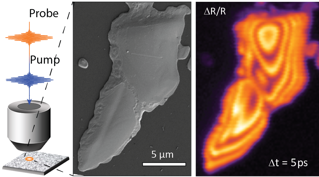
Time-resolved microscopies provide the ability to spectroscopically probe sub-micron spots in functional materials. Here, the shape of a CsPbBr3 domain leads to the Fabry-Perot interference pattern seen in the image at right - a similar effect that causes the rainbow sheen of a thin oil layer on water.
The electronic structure of functional materials is strongly coupled to both physical structure and chemical composition. As a result, microscopic variation in either parameter (aka defects) can have profound influence on the optical, electrical, and photocatalytic properties of the material. Sometimes these defects can degrade functionality; sometimes they can improve functionality.
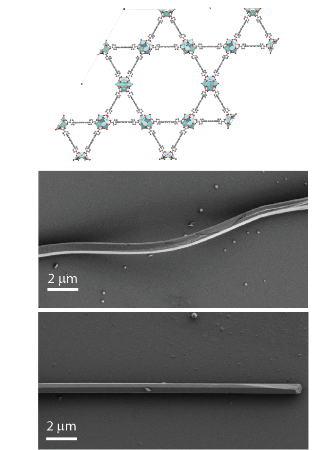
At right are SEM images of single crystals of the metal organic framework PCN-222. The bend seen in middle image is indicative of accumulated point defects introduced during the grown of the particles. We use optical microscopies to ask simple questions about these types of systems: How do excited state lifetimes change in the region of the bend? Are their changes in the excited state branching ratio introduced by the higher defect density? Can we design strategies to reduce or enhance defect concentration to achieve improved functionality?
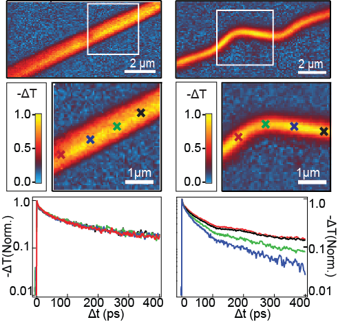 The data shown at left illustrates how time-resolved microscopy can help answer these
questions. At the top is a comparison of two pump-probe images of two PCN-222 crystals,
like those shown in the SEM above. The middle row shows the same two crystals, but
zoomed in to the regions highlighted by the white boxes. The "contrast" of the images
is determined by the pump-induced change in complex index of refraction, which in
turn causes changes to the absorptivity and reflectivity of the crystals.
The data shown at left illustrates how time-resolved microscopy can help answer these
questions. At the top is a comparison of two pump-probe images of two PCN-222 crystals,
like those shown in the SEM above. The middle row shows the same two crystals, but
zoomed in to the regions highlighted by the white boxes. The "contrast" of the images
is determined by the pump-induced change in complex index of refraction, which in
turn causes changes to the absorptivity and reflectivity of the crystals.
The "x" indicators on the middle images show regions where excited state decay kinetics were collected with a spatial resolution of ~ 400 nm. The traces shown below are correspondingly color coded, and indicate how quickly the excited state decays at each location. In the straight crystal, the excited state lifetime is the same from one location to the next, but in the bent crystal, the lifetimes vary significantly throughout the bend. This variability in lifetime reflects the influence local structural defects have on the relaxation of photogenerated excited states. Such measurements enable structure-function correlations with precision that is out of reach to conventional spectroscopic probes and pave the way for the next generation of intentionally designed functional materials.
Advancing Time-Resolved Microscopy
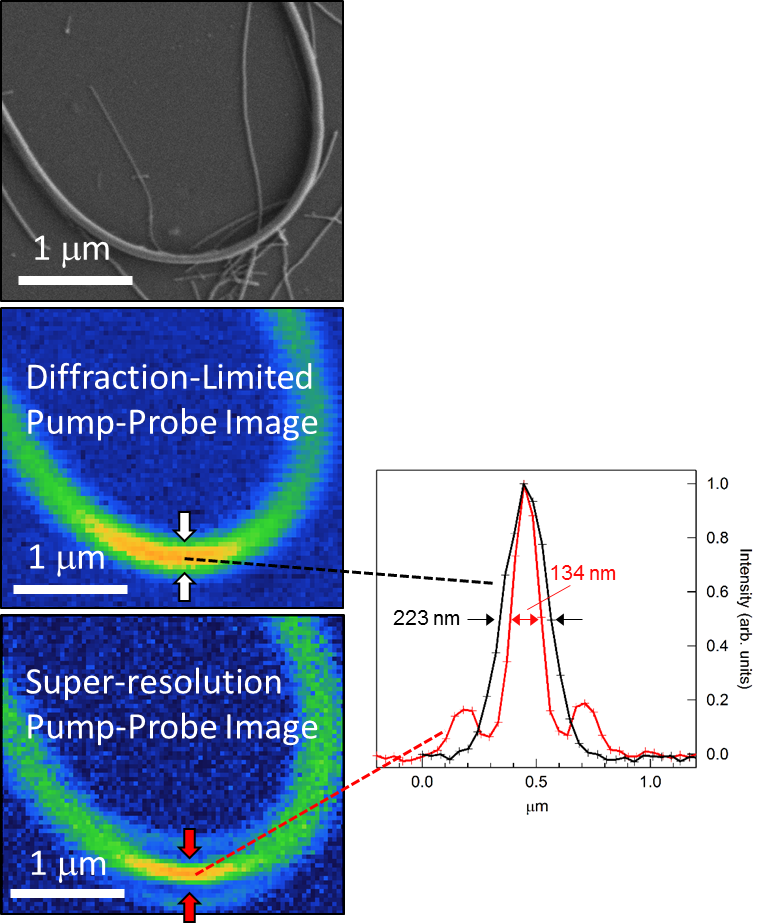
Super-resolution pump-probe images: The diffraction limited image at t = 0 ps gives a ~ 220 nm linewidth, whereas the super-resolution is much narrower (134 nm).
We actively developing new methods to enable spectroscopic probes with better spatial resolution, higher sensitivity, and more spectral information. Work in our group has spanned the development of super-resolution pump-probe microscopy, which enables the interrogation of material optoelectronic properties on smaller length scales, to the development of time-resolved broadband microscopy techniques. Our current efforts are aimed at improving pump-probe sensitivity and further leveraging correlative microscopies.